Circuit Board Design Service: A Complete Guide from Concept to Production
22 Sep, 2026
12 Views 0 Like(s)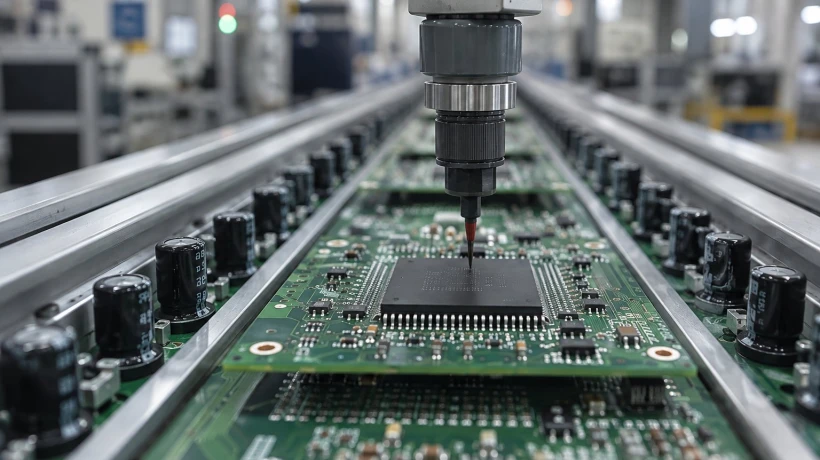
The process bridges creative engineering with precise manufacturing standards, ensuring your PCB performs reliably in the final product. This guide walks through every critical phase of a circuit board design service from the first requirements discussion to the final production handoff.
A circuit board design service takes your product idea through every technical stage from defining electrical requirements and drawing schematics to laying out components, running design verification, and generating manufacturing-ready output files. The process bridges creative engineering with precise manufacturing standards, ensuring your PCB performs reliably in the final product.
If you are a product developer, startup founder, or electronics engineer, understanding this journey helps you make smarter decisions, avoid costly redesigns, and bring better products to market faster. This guide walks through every critical phase of a circuit board design service from the first requirements discussion to the final production handoff.
What Does a Circuit Board Design Service Actually Cover?
Many clients assume PCB design is simply "drawing a board." In reality, it spans multiple engineering disciplines electrical design, signal integrity, thermal management, mechanical constraints, and design-for-manufacturability (DFM). A full-service provider handles all of these under one workflow.
Here is what a comprehensive service typically includes:
-
Requirements gathering and feasibility review
-
Schematic capture and netlist generation
-
Component selection and sourcing verification
-
PCB layout and routing
-
Design rule checks (DRC) and electrical rule checks (ERC)
-
Gerber file generation and manufacturing documentation
Phase 1: Requirements Gathering and Feasibility
Every strong PCB design starts with a detailed requirements brief. This includes power specifications, signal types, operating environment, mechanical form factor, regulatory needs, and target cost. Skipping this phase is one of the most common reasons designs go through expensive revision cycles.
During feasibility review, the design team checks whether your functional requirements can be achieved within your physical and budget constraints. For example, if you need a compact IoT sensor that operates in high-humidity environments, the board material selection, coating requirements, and connector choices all get evaluated at this stage not after layout is complete.
Why Requirements Documentation Prevents Costly Rework
A change at the schematic stage costs a fraction of what the same change costs at the prototyping stage. Capturing clear functional, mechanical, and compliance requirements upfront compresses the total design cycle and protects your development budget.
Phase 2: Schematic Design and Component Selection
The schematic is the logical blueprint of your circuit. It defines how every component connects power rails, signal paths, ground references, protection circuitry, and interfaces. A well-drawn schematic is not just a technical document; it is the communication bridge between design and manufacturing teams.
Component selection happens in parallel. Engineers evaluate parts based on availability, lead time, cost, and reliability. In Singapore's electronics manufacturing ecosystem, component procurement is tightly linked to regional supply chains so verifying component availability before committing to a design is essential, not optional.
Key Considerations in Component Selection
-
Lifecycle status: Avoid components already in end-of-life (EOL) phase
-
Package compatibility: Ensure the footprint matches your manufacturing capabilities
-
Second-source options: Identify alternative suppliers to reduce supply risk
-
Regulatory compliance: Confirm RoHS, REACH, or other applicable standards
Phase 3: PCB Layout and Routing
This is where the PCB design process becomes highly technical and where experience matters most. The layout engineer translates the schematic into a physical board placing components, routing copper traces, managing layer stackups, and handling impedance-controlled signals.
Poor layout decisions create problems that no amount of software simulation can fully predict: EMI emissions, crosstalk between signal lines, thermal hotspots, and power integrity issues. High-speed digital designs, RF circuits, and power electronics each require different layout strategies.
Critical Layout Rules That Affect Performance
|
Design Area |
Common Mistake |
Best Practice
|
|---|---|---|
|
Decoupling capacitors |
Placed too far from IC power pins |
Place as close as possible to reduce inductance |
|
Ground planes |
Split or fragmented ground |
Use solid, uninterrupted ground reference planes |
|
High-speed traces |
Inconsistent trace lengths |
Length-match differential pairs and clock lines |
|
Thermal management |
No thermal relief on power components |
Add thermal vias and copper pours for heat dissipation |
Phase 4: Design Verification and Review
Before any files go to fabrication, the design must pass multiple verification layers. This is not a formality — it is the stage that catches errors that would otherwise result in non-functional prototypes or field failures.
Verification in a professional custom PCB design workflow includes:
-
Design Rule Check (DRC): Confirms trace widths, clearances, and via sizes meet fabrication tolerances
-
Electrical Rule Check (ERC): Validates the netlist for unconnected pins, power conflicts, and signal errors
-
Signal integrity simulation: Models how high-speed signals behave across the board
-
Thermal analysis: Identifies components or areas at risk of overheating under load
-
DFM review: Checks that the design can be manufactured reliably at your target volume and yield
What Is a Design for Manufacturability (DFM) Review?
A DFM review evaluates your design against the real-world capabilities of the fabrication and assembly process. It flags issues like insufficient solder mask clearance, pad sizes incompatible with pick-and-place machines, or via placement that complicates automated optical inspection (AOI). Catching these issues before production prevents costly tooling changes and assembly failures.
Phase 5: Gerber Files and Production Documentation
Once verification is complete, the design is exported into manufacturing output files. The Gerber format (RS-274X) is the industry standard for PCB fabrication data. These files define every copper layer, solder mask, silkscreen, and drill location on the board.
A complete production package also includes:
-
Bill of Materials (BOM) with manufacturer part numbers
-
Assembly drawings and component placement files (Centroid/Pick-and-Place files)
-
Drill files and impedance stack-up documentation
-
Test specifications and inspection criteria
Submitting incomplete or inconsistent documentation is one of the leading causes of fabrication delays. A professional PCB design service delivers a complete, verified package that the fab house can act on without back-and-forth clarification.
How to Evaluate a PCB Design Service Provider
Not all providers offer the same depth of capability. When assessing a partner, look beyond software tools and focus on process maturity, domain experience, and production integration.
Questions worth asking:
-
Do they have experience with your product category (medical, industrial, consumer, RF)?
-
Can they support both prototype quantities and volume production?
-
Do they offer in-house DFM reviews tied to their manufacturing capabilities?
-
What verification tools and simulation software are used?
-
Can they manage component sourcing and supply chain integration?
For startups in particular, choosing a provider with integrated design-to-manufacturing capabilities reduces handoff friction and shortens time to first prototype significantly.
Circuit Board Design for Startups: What to Expect
If you are bringing a hardware product to market for the first time, the PCB design process can feel opaque. Here is a realistic timeline and what each phase delivers:
|
Phase |
Typical Duration |
Key Deliverable
|
|---|---|---|
|
Requirements and feasibility |
1–3 days |
Design brief and scope agreement |
|
Schematic design |
3–7 days |
Reviewed schematic and BOM draft |
|
PCB layout |
5–10 days |
Routed board with layer stackup |
|
Verification and review |
2–4 days |
DRC/ERC reports, DFM sign-off |
|
Production file generation |
1–2 days |
Complete Gerber and assembly package |
Timelines vary based on design complexity, revision cycles, and component availability. A simple two-layer board for a consumer device moves faster than a multilayer, high-speed embedded system.
Conclusion
A well-executed circuit board design service is not just a technical task it is a structured engineering process that directly determines whether your product performs reliably, passes compliance testing, and reaches production on schedule. Every phase, from requirements capture to Gerber output, builds on the one before it. Shortcuts at any stage compound into larger problems downstream.
For product developers and engineers in Singapore looking for a partner who combines design expertise with manufacturing integration, Statron offers PCB design services built around production-ready outcomes not just finished files.
Frequently Asked Questions
What is included in a professional circuit board design service?
A professional circuit board design service typically covers schematic capture, component selection, PCB layout and routing, design rule checks, signal integrity review, and full production file generation including Gerbers, BOM, and assembly documentation.
How long does the PCB design process take from start to finish?
For a standard design, the PCB design process takes between two to four weeks, covering schematic design, layout, verification, and file output. Complex multilayer or high-speed designs with multiple revision cycles can extend this timeline further.
What is a DFM review and why does it matter?
A Design for Manufacturability (DFM) review checks that your PCB layout is compatible with fabrication and assembly processes. It prevents production failures caused by incorrect pad sizes, clearance violations, or features that automated assembly equipment cannot reliably handle.
What files do I receive at the end of a custom PCB design project?
At project completion, you receive Gerber files for fabrication, a Bill of Materials with part numbers, pick-and-place files for assembly, drill files, and an assembly drawing everything a contract manufacturer needs to build your board without additional clarification.
Can a PCB design service help with component sourcing?
Yes, many providers integrate component sourcing into the design workflow. They verify part availability and lead times during schematic design and identify alternative components to reduce supply chain risk before the design is finalised.
What should startups look for when choosing a PCB design partner?
Startups should prioritise providers with integrated design-to-manufacturing capability, domain experience in their product category, transparent revision policies, and DFM review processes tied directly to production this reduces prototype failures and accelerates the path to volume manufacturing.



Comments
Login to Comment